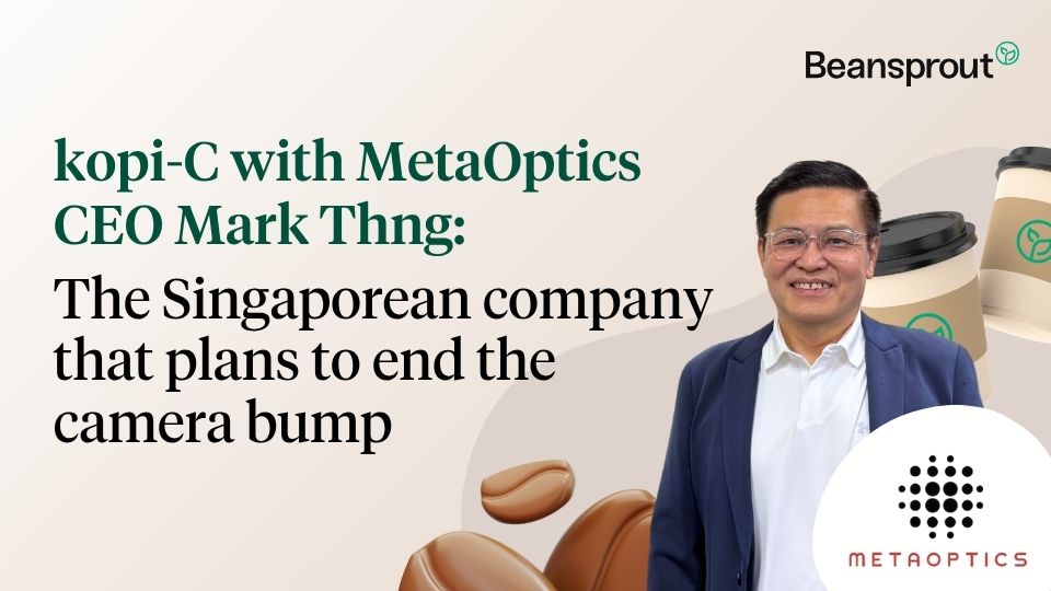
kopi-C with MetaOptics CEO Mark Thng: the Singaporean company that plans to end the camera bump
Stocks
Powered by
By Julian Wong • 05 Nov 2025
Why trust Beansprout? We’ve been awarded Best Investment Website at the SIAS Investors’ Choice Awards 2025
'%3e%3cpath%20fill-rule='evenodd'%20clip-rule='evenodd'%20d='M17.64%209.20455C17.64%208.56637%2017.5827%207.95273%2017.4764%207.36364H9V10.845H13.8436C13.635%2011.97%2013.0009%2012.9232%2012.0477%2013.5614V15.8195H14.9564C16.6582%2014.2527%2017.64%2011.9455%2017.64%209.20455V9.20455Z'%20fill='%234285F4'/%3e%3cpath%20fill-rule='evenodd'%20clip-rule='evenodd'%20d='M9%2018C11.43%2018%2013.4673%2017.1941%2014.9564%2015.8195L12.0477%2013.5614C11.2418%2014.1014%2010.2109%2014.4205%209%2014.4205C6.65591%2014.4205%204.67182%2012.8373%203.96409%2010.71H0.957275V13.0418C2.43818%2015.9832%205.48182%2018%209%2018V18Z'%20fill='%2334A853'/%3e%3cpath%20fill-rule='evenodd'%20clip-rule='evenodd'%20d='M3.96409%2010.71C3.78409%2010.17%203.68182%209.59318%203.68182%209C3.68182%208.40682%203.78409%207.83%203.96409%207.29V4.95818H0.957273C0.347727%206.17318%200%207.54773%200%209C0%2010.4523%200.347727%2011.8268%200.957273%2013.0418L3.96409%2010.71V10.71Z'%20fill='%23FBBC05'/%3e%3cpath%20fill-rule='evenodd'%20clip-rule='evenodd'%20d='M9%203.57955C10.3214%203.57955%2011.5077%204.03364%2012.4405%204.92545L15.0218%202.34409C13.4632%200.891818%2011.4259%200%209%200C5.48182%200%202.43818%202.01682%200.957275%204.95818L3.96409%207.29C4.67182%205.16273%206.65591%203.57955%209%203.57955V3.57955Z'%20fill='%23EA4335'/%3e%3c/g%3e%3cdefs%3e%3cclipPath%20id='clip0_0_2849'%3e%3crect%20width='18'%20height='18'%20fill='white'/%3e%3c/clipPath%3e%3c/defs%3e%3c/svg%3e)
Make Beansprout your preferred source on Google
Add us on Google to see more of our insights in your search results
MetaOptics CEO Mark Thng shares how they are using semiconductor technology to create flat, glass-based metalenses to create everything from non-contact fingerprint scanners to optical AI chips.
Mobile phones get thinner, sleeker, and lighter every few years. Yet no matter how slim the design, one feature remains, seemingly impossible for manufacturers to smooth away: the awkward camera “bump”.
These protruding lenses are a physical reminder of the limits of existing injection moulded polymer optical engineering.
MetaOptics, a Singapore-based semiconductor optics company, wants to change this. Its team is developing metalenses—flat, glass-based lenses built and fabricated using the same technology and manufacturing process as semiconductor chips.
Unlike conventional polymer lenses that warp under heat, MetaOptics’ lenses are fabricated on glass, making them both smaller and more heat-resistant. The result is an optical module that’s just two millimetres thick, with an actual metalens thickness of 0.775mm, capable of sitting flush against a phone’s back while still featuring reasonable performance.
MetaOptics CEO Mark Thng highlights this, calling out how brands publicise thinness without mentioning the protruding camera. “We are hoping to solve this,” he says. At the same time, the company’s ambitions go far beyond fixing a camera bump.
For us, we’re not trying to compete in cost. We’re trying to jump way ahead to breakthrough existing optics technologies and miniaturising smart devices with our thin metalenses.
Beyond the bump: a lens that thinks like a chip
To understand MetaOptics' business, one must first understand its technology.
Firstly, MetaOptics’ lenses sound more like chips than optical parts precisely because they are. Instead of using curved glass, the company uses semiconductor photolithography processes to directly etch millions of microscopic pillars on a flat wafer—similar to how transistors are etched onto silicon. The smallest features measure 80 nanometres, one-thousandth the width of a human hair.
Secondly, this manufacturing method allows their lenses to potentially possess a unique quality: they can behave like programmable optical surfaces.
“Because metalens is dielectric in nature, we actually can put certain voltage to the lens and the reflective index will change,” Thng explains.
In practice, that means one lens can adapt to perform multiple roles—zooming, focusing, or shifting depth—without the need for multiple cameras.
“We call the camera that we produce a computational camera,” he says. “We can actually change it to do certain things.”
Instead of five fixed lenses doing separate jobs, Thng envisions a single, tuneable one. The result could reduce cost, save space, and make devices slimmer than ever.
“People are used to comparing apples to oranges,” he adds with a grin. “For us, we’re not trying to compete in cost. We’re trying to jump way ahead to breakthrough existing optics technologies and miniaturising smart devices with our thin metalenses.”

From phones to fingerprints and AI chips
While smartphones are the most visible frontier, MetaOptics’ technology has broader implications. One of its most intriguing applications lies in 3D biometrics.
In today’s airports, banks, homes and offices, fingerprint scanners still require a firm press against a glass panel. For Thng, this is a process that’s both unhygienic and insecure.
“Those devices are not guaranteed,” he explains. “Security is low … if you are a private investigator, you will find that I can copy your fingerprint because you leave your fingerprint there.”
His team’s solution is a non-contact 3D fingerprint scanner that uses light to map prints without physical touch. “To avoid all those touching panels,” he shares, “I said okay, let me make it non-contact, and we were able to do it.”
The company is now working with universities in Hong Kong and Korea-based fingerprint device companies to explore the possibility of integrating the technology into ATM machines as well as 3D Biometrics sensors, particularly for elderly users who struggle with PIN codes or forget their cards.
MetaOptics is also pushing into AI hardware, an area few optics companies dare to enter. By embedding metalenses directly into chip packaging—a process known as Co-Packaged Optics (CPO)—MetaOptics can replace copper wiring with light-based data transmission.
“We use light to transmit, so you can eliminate the use of copper, and go into light-based transmission,” Thng explains. “Then the chip will be smaller, emit less heat, and cost less because you’ve got less circuitry inside.”
It’s heartening to see international investors take notice of what we’re building here ... We’re very grateful for their confidence, and we hope to keep creating value as we grow.
The lean entrepreneur behind the lens
Unlike many other start-ups, MetaOptics’ story began with its founder’s retirement.
“I retired in 2018. Financially, I’m free,” says Thng. “I became a consultant to some companies that were made up of founders who are very young … I saw VCs investing in them, but for many, the money just goes to waste.”
Those experiences convinced him that there was a better way to build deep-tech businesses. His philosophy: stay lean, stay disciplined, and always focus on the return to shareholders.
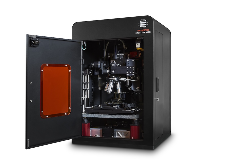
MetaOptics began its initial foray into the industry as an equipment maker, developing and producing compact laser writers for research labs. Those early machines funded the company’s R&D and proved that its technology could move from lab to market.
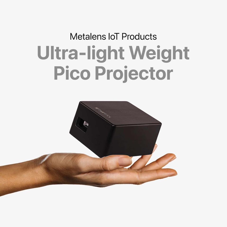
Today, the company designs and fabricates its own metalenses and imaging modules, including a portable projector that plugs directly into smartphones. “It takes power from an iPhone or Android phone,” he says. “[It’s bright enough that] I use it to watch TV movies when I’m lying on my bed at night.”
Even the World Intellectual Property Organisation (WIPO) ordered one after a visit. “They came here, they interviewed us, then the lady went back to Geneva and then she went to our Shopify and ordered. So we shipped it to her.”
MetaOptics remains small but nimble. For FY2024, the company reported revenue of S$79,440 and a net loss of about S$2.3 million. In the first quarter of FY2025, net loss was approximately S$706,000.
When the time came to raise capital, Thng chose to list locally in Singapore.
We believe we will be a unicorn ... Based on the technology and our sensing of the market, I think we are running as fast as we can.
For Thng, the decision to list at home carried both strategic and sentimental weight. “I see many people going overseas … and I saw the industry and the landscape of our stock exchange not doing very well. So I thought maybe we can try to contribute at least.”
The listing—30 million shares at S$0.20 each—raised S$6.0 million in gross proceeds (about S$4.0 million net of expenses) on SGX’s Catalist board in September 2025, giving MetaOptics the credibility to compete globally.
At its debut, the company was valued at roughly S$47 million, with shares surging 25 per cent on the first day of trading. By early October 2025, MetaOptics’ market capitalisation has more than doubled to over S$110 million.
Thng says the listing also underscores how far SGX can reach. The Catalist debut drew strong interest from both institutional and retail investors, as well as several based overseas. Among them was Miss Yvonne Zhao Yi Qing, a Singapore-based foreign investor who runs her own investment firm and participated in the fund-raising.
“It’s heartening to see international investors take notice of what we’re building here,” he says. “We’re very grateful for their confidence, and we hope to keep creating value as we grow.”
For him, this is an encouraging sign that SGX’s platform can give even young deep-tech companies with the right set-up and ambitions global visibility.
Running fast, staying grounded
For a man who started his company post-retirement, Thng sounds like someone just getting started.
“We believe we will be a unicorn,” he says, matter-of-factly. “Based on the technology and our sensing of the market, I think we are running as fast as we can. I think we are way ahead of everyone.”
Yet he’s also candid about the challenges of building deep-tech ventures in Singapore. His hope is that MetaOptics’ success might change that.
“After MetaOptics’ success, [VCs and investors] can pay more attention to Singapore, and to entrepreneurs wanting to list on SGX. Maybe they can be more supportive of us,” he says.
Despite some frustrations, Thng remains hopeful.
“We have a few thousand PhDs just across the road at our National Institute & universities. We have many wonderful technologies,” he says. “If two thousand PhDs can spin off, that’s two thousand Catalist companies possibly listing.”
It’s a fitting vision for a company that started with the simple vision of flattening a camera lens.
About MetaOptics
MetaOptics Ltd (Catalist: 9MT) is a leading-edge semiconductor optics company pioneering glass-based metalens solutions enhanced by AI-driven image processing. Using advanced optical design and a scalable 12-inch DUV lithography process, it powers next-generation applications in CPO, mobile, AR VR, automotive and other emerging markets. Headquartered in Singapore, MetaOptics aims to deliver high-performance optics with the reliability and scalability demanded by today's most innovative technology brands.
As of 27th Oct 2025, MetaOptics has successfully incorporated its subsidiary, MetaOptics Inc. (USA), in the United States of America with the goal to expand globally and engage strategic world class customers with their metalens. They are installing their Direct Laser Writers in these regions to enable fast prototyping of the metalens for customers’ evaluation. They are exploring many possibilities in the USA, including the mass production of the metalens.
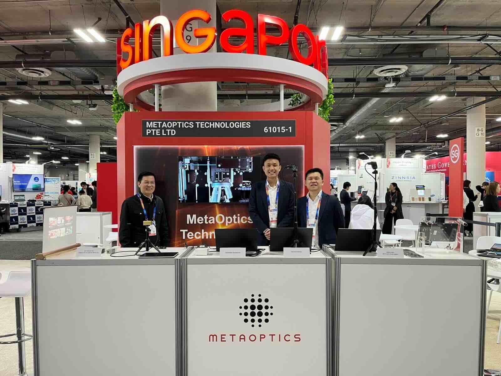
They will also be participating in CES 2026 from January 6th – 9th in Las Vegas, USA. With recently completed manufacturing of 12” glass wafers of their 5 mega pixel colour imaging rectangular metalens, they are now able to make lab images look sharper with much better resolution than their previous round metalens.
A generation 2 thinner Pico Projector is also in process. Printed circuit boards are in assembly and they expect samples to be ready for launching at CES 2026. In particular, they will also be demonstrating their technology through their 5G Metalens Smart Phone prototype. The AI phone is 6mm thin without the metalens camera protruding out of the casing, and feature both the colour imaging metalens camera and a 3D non-contact fingerprint sensor.
About kopi-C: the Company brew
kopi-C is a regular column by SGX Research in collaboration with Beansprout, a MAS-licensed investment advisory platform, that features C-level executives of leading companies listed on SGX. These interviews are profiles of senior management aimed at helping investors better understand the individuals who run these corporations.
Read also
Gain financial insights in minutes
Subscribe to our free weekly newsletter for more insights to grow your wealth
Most Popular

Comments
0 comments